PMI Inspection System Overview (Probe Mark Inspection)
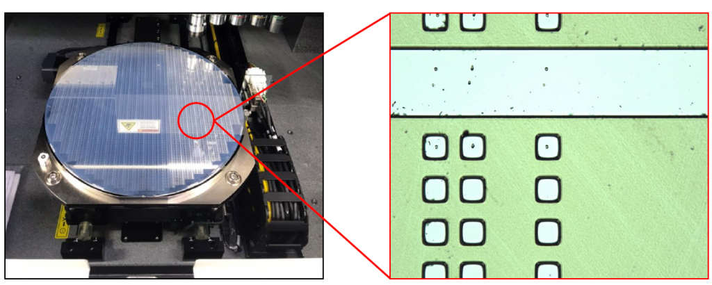
This equipment inspects the size and location of Probe Marks on Wafer PADs to evaluate the contact characteristics of the Probe Card.
Unlike conventional sample inspection or visual inspection, it can inspect all PADs on a wafer in a short time, identifying the pattern and behavior of contact marks.
Furthermore, by analyzing PMI Data, it helps improve the quality of the Probe Card.
By analyzing the length of Contact Scrub Marks, it is possible to check for needle tip breakage after testing.
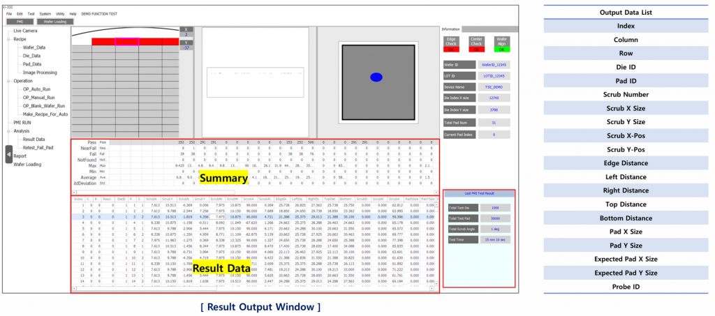
Inspection results can be exported as CSV files and submitted to the customer as reports.
PMI(Probe Mark Inspection) 장비사양
Item
Specification
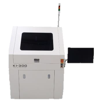
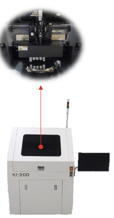
Machine Name
WI-300 (*Formerly KI-300)
Measurement Time (12inch / 10,000 Pins)
≤15 minutes (Used Mid) *Time may vary depending on PAD shape/location
Measurement Method
Area Confocal
Precision
Pixel Size: 1 μm, Resolution: ≤1 μm
Lighting
Standard
High-Speed Focus
Standard
Tool-to-tool Correlation
Standard
On-the-fly Image Capture
Standard (Mono)
Full Wafer Color Image Capture
Standard (Color)
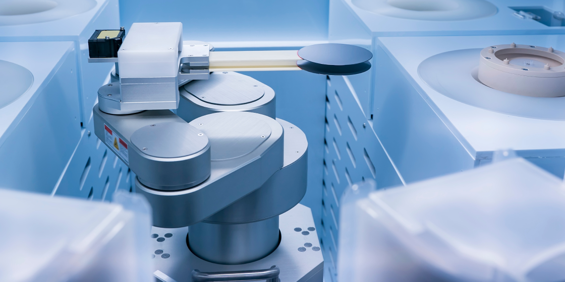
Turret Assembly
Linear turret (4-position)
Supports 8-inch and 12-inch wafers
Enables post-analysis of PMI data even after test completion and retesting of failed data
User-friendly operation, PMI result data generation supported
Enables post-analysis of PMI data even after test completion and retesting of failed data
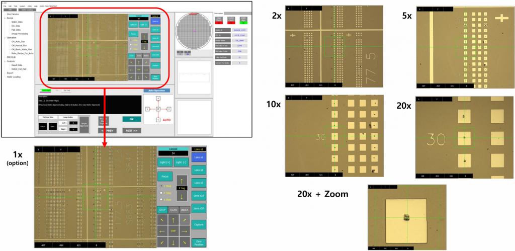
Supports a variety of lens combinations (1X*, 2X, 5X, 10X, 20X)
Data backup supported (Hard Disk Mirroring)
Capable of automatic movement to pre-defined PAD positions
Objective Lenses & Field of View (FOV):
Magnification
1X (Option)
2X
5X
10X
20X
FOV (mm)
8.0 × 6.0
4.0 × 3.0
1.6 × 1.2
0.8 × 0.6
0.4 × 0.3
Equipment Setup Types
Device Setting [Type 1]
Wafer Map provided through Live Vision
Test / Untested Die settings
PAD Data generation
📌 [Create Wafer Map]
Device Setting [Type 2]
Probe Card Data loading
No Wafer Map or PAD Data generation
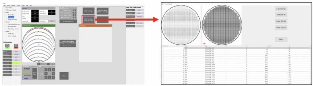
📌 [Create Wafer Map from Card Data]
This explanation compares two types of device setting methods (Type 1 and Type 2).
Type 1 involves manually creating a wafer map and collecting pad information,
while Type 2 automatically generates the wafer map based on the data stored in the probe card.
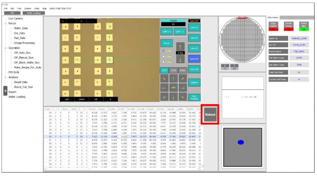
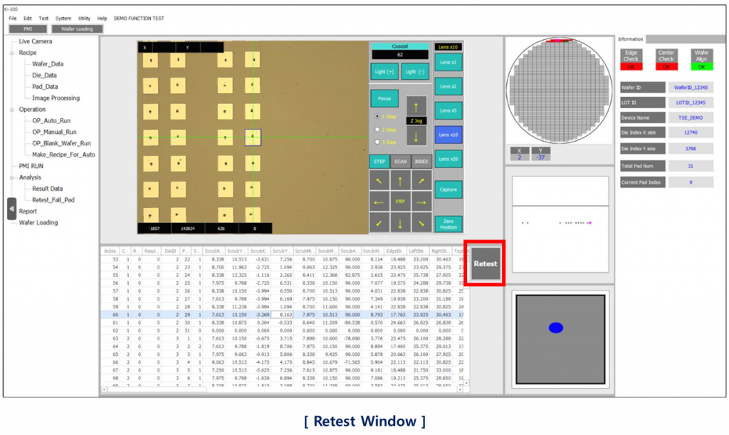
Retest Function
Online retesting is available for all failed results or selected PADs.
Retesting can be performed by comparing previous inspection results with the actual wafer.
DATA 시트 / Retest 기능
PMI 결과 데이터 (20종) 출력 및 요약 Fail 결과 전체 또는 선택된 Pad에 대한 Online Retest 가능 기존 결과 Data들을 불러오고, 실제 Wafer와 비교 및 Retest 가
확대 배율
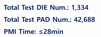
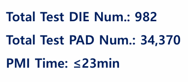
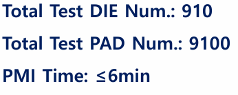
PAD 위치 및 형상에 따른 PMI 시간
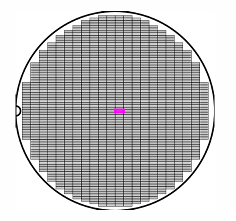
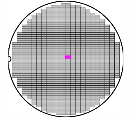
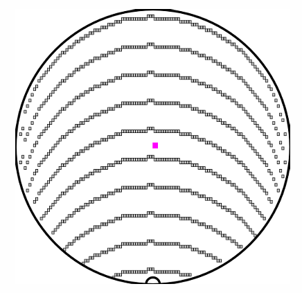
Wafer Size : 12inch Wafer
Probe Card Type : Memory Probe Card
GSTT
B128 (Basement 1), 51-9, Dongtan Cheomdan Sandan 1-ro, Hwaseong-si, Gyeonggi-do, Republic of Korea P.H : Tel) +82-10-5142-4671 | CEO : Kim Taewoo | E-mail address : taeug260@global-stt.com